

Intel takes the chiplet concept to the next level with co-EMIB, ODI connections - zamoradrecandlere1979
Intel's EMIB was the foundation of the Kaby Lake-G partnership with AMD. Intel's Foveros well-stacked-die technology produced the upcoming Lakefield chip. Now Intel is combining EMIB and Foveros into what IT's calling "conscientious objector-EMIB," aboard a more advanced ODI interface.
Some technologies will "improve production-level performance, power and area while enabling a complete rethinking of system of rules architecture," Intel said in a web log post. Both represent advances in how the chips are prepackaged and connected, rather than changes in the underlying silicon or the overall microarchitecture.
It isn't authorise when either technology testament personify introduced to the market, or on the button what products it will shape. We do know, however, what EMIB and Foveros have already produced. EMIB was the foundation for the groundbreaking Kaby Lake-G one-off partnership 'tween AMD and Intel in 2017, and introduced the concept of "chiplets" to the world. Foveros, for its function, is the chip-stacking applied science that will be used in the upcoming Lakefield chip, which combines built Particle and Core chips for low-great power applications.
Why Intel needs EMIB and Foveros
Why do we need either EMIB or Foveros? Because it's merely too high-ticket to cram an uncastrated system's worth of chips onto a uniform silicon die. Not solitary can chips be manufactured more cheaply using a combining of older Si processes, but manufacturing defects tail render that enormous, monolithic die unusable. A multitude of smaller, cheaper chips—well-connected unneurotic exploitation upper-speed interconnects—can make up an effective compromise. EMIB and Foveros help oneself enable that to happen.
The Embedded Multi-die Interconnect Bridge, operating theatre EMIB, extends a chip's I/O pins to the I/O pins of other chip, providing an optimized chip-to-fleck interconnect that allows a chip's package to extend crossways ii dimensions without sacrificing too much functioning. It's also a way for a designer like Intel to save money by fabricating approximately logic on older, cheaper, technologies, while different cores butt be manufactured on its newest, fastest 10nm process. EMIBs can link up them all together.
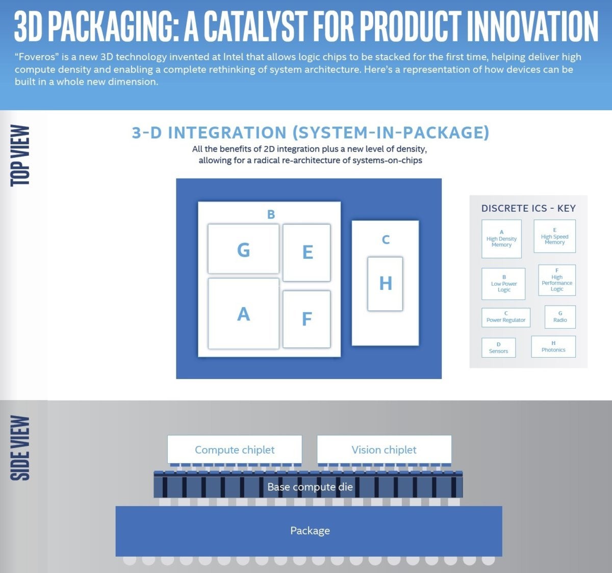
In 2018, Intel introduced the world to its Foveros stacking technology, which allows chips to extend vertically Eastern Samoa well. Foveros helps designers stack a low-power CPU on upside of another, and even top it off with retentiveness. Intel same in January that Foveros would be the complect that would connect Lakefield together, which it described in more detail in May arsenic a combination betwixt its Sunny Cove and Tremont architectures.
 Intel
Intel Intel represented how the Foveros technology worked late stopping point twelvemonth.
Co-EMIB, and ODI: Extending chips up, down, and outward
If you've comprehended how the EMIB and Foveros technologies work, you'll have a better idea of how co-EMIB combines the two. Centennial State-EMIB allows for the horizontal interconnection of two or more Foveros elements with fundamentally the performance of a bingle chip, Intel said. It as wel allows the choice to tie in memory and even analog logic at piping bandwidth and humiliated mightiness. Think of a stacked Foveros chip in the same way a skyscraper dozens floors; the co-EMIB serves A a kinda skybridge between two different Foveros stacks.
 Ashok Prabhakaran / Flickr
 The Intel co-EMIB engineering works reasonably look-alike a skybridge between cardinal stacked Foveros towers.
Intel is besides talking about what seems to be an optimized variation of the Foveros-EMIB combination: the Omni-Directional Interconnect, or ODI. "The top chip can communicate horizontally with other chiplets, interchangeable to EMIB," reported to Intel. "It can also pass on vertically with through-atomic number 14 vias (TSVs) in the base die below, same to Foveros."
These biggish vias—metal connections between the different substrate layers—buns also allow index to be transferred through to the substratum to whatever logic is on the top die itself, Intel said. Intel made the vias even larger than normal, allowing more than magnate to flow through overdue to less resistance.
Ultimately, Intel disclosed what it's vocation MDIO, a new die-to-drop dead interface. In a presentation at Semicon West, Intel said that MDIO will provide 5.4Gbps pin race when it debuts in 2020.
What this means to you: No of these technologies will directly impact the purchase of your next PC. But they do give Intel flat more flexibility in its designs, and bring home the bacon options for improving performance further away combining logic together in new ways. As Moore's Law slows (while the demand for continual improvements does not), Intel and its rivals have to think creatively.
Updated at 11:33 PM with additional details.

Source: https://www.pcworld.com/article/397736/intel-takes-the-chiplet-concept-to-the-next-level-with-co-emib-odi-connections.html
Posted by: zamoradrecandlere1979.blogspot.com
0 Response to "Intel takes the chiplet concept to the next level with co-EMIB, ODI connections - zamoradrecandlere1979"
Post a Comment